Sure... Read the articlesOriginally Posted by Lucas


 NIII
NIII
Sure... Read the articles
NIII
http://web.mit.edu/newsoffice/2013/p...sion-0418.html
Special deal on photon-to-electron conversion: Two for one!
New technique developed at MIT could enable a major boost in solar-cell efficiency.
David L. Chandler, MIT News Office
Throughout decades of research on solar cells, one formula has been considered an absolute limit to the efficiency of such devices in converting sunlight into electricity: Called the Shockley-Queisser efficiency limit, it posits that the ultimate conversion efficiency can never exceed 34 percent for a single optimized semiconductor junction.
Now, researchers at MIT have shown that there is a way to blow past that limit as easily as todays jet fighters zoom through the sound barrier which was also once seen as an ultimate limit.
Their work appears this week in a report in the journal Science, co-authored by graduate students including Daniel Congreve, Nicholas Thompson, Eric Hontz and Shane Yost, alumna Jiye Lee 12, and professors Marc Baldo and Troy Van Voorhis.
The principle behind the barrier-busting technique has been known theoretically since the 1960s, says Baldo, a professor of electrical engineering at MIT. But it was a somewhat obscure idea that nobody had succeeded in putting into practice. The MIT team was able, for the first time, to perform a successful proof of principle of the idea, which is known as singlet exciton fission. (An exciton is the excited state of a molecule after absorbing energy from a photon.)
In a standard photovoltaic (PV) cell, each photon knocks loose exactly one electron inside the PV material. That loose electron then can be harnessed through wires to provide an electrical current.
But in the new technique, each photon can instead knock two electrons loose. This makes the process much more efficient: In a standard cell, any excess energy carried by a photon is wasted as heat, whereas in the new system the extra energy goes into producing two electrons instead of one.
While others have previously split a photons energy, they have done so using ultraviolet light, a relatively minor component of sunlight at Earths surface. The new work represents the first time this feat has been accomplished with visible light, laying a pathway for practical applications in solar PV panels.
This was accomplished using an organic compound called pentacene in an organic solar cell. While that materials ability to produce two excitons from one photon had been known, nobody had previously been able to incorporate it within a PV device that generated more than one electron per photon.
Our whole project was directed at showing that this splitting process was effective, says Baldo, who is also the director of the Center for Excitonics, sponsored by the U.S. Department of Energy. We showed that we could get through that barrier.
The theoretical basis for this work was laid long ago, says Congreve, but nobody had been able to realize it in a real, functioning system. In this system, he says, everyone knew you could, they were just waiting for someone to do it.
This is the landmark event we had all been waiting to see, adds Richard Friend, the Cavendish Professor of Physics at the University of Cambridge, who was not involved in this research. This is really great research.
Since this was just a first proof of principle, the team has not yet optimized the energy-conversion efficiency of the system, which remains less than 2 percent. But ratcheting up that efficiency through further optimization should be a straightforward process, the researchers say. There appears to be no fundamental barrier, Thompson says.
While todays commercial solar panels typically have an efficiency of at most 25 percent, a silicon solar cell harnessing singlet fission should make it feasible to achieve efficiency of more than 30 percent, Baldo says a huge leap in a field typically marked by slow, incremental progress. In solar cell research, he notes, people are striving for an increase of a tenth of a percent.
Solar panel efficiencies can also be improved by stacking different solar cells together, but combining solar cells is expensive with conventional solar-cell materials. The new technology instead promises to work as an inexpensive coating on solar cells.
The work made use of a known material, but the team is now exploring new materials that might perform the same trick even better. The field is working on materials that were chanced upon, Baldo says but now that the principles are better understood, researchers can begin exploring possible alternatives in a more systematic way.
Christopher Bardeen, a professor of chemistry at the University of California at Riverside who was not involved in this research, calls this work very important and says the process used by the MIT team represents a first step towards incorporating an exotic photophysical process (fission) into a real device. This achievement will help convince workers in the field that this process has real potential for boosting organic solar cell efficiencies by 25 percent or more.
The research was performed in the Center for Excitonics and supported by the U.S. Department of Energy. MIT has filed for a provisional patent on the technology.
ILLUSTRATION: CHRISTINE DANILOFF/MIT
NIII
http://gizmodo.com/5995046/graphene-has-a-fatal-flaw
Graphenes Achilles Heel
Jamie Condliffe
Graphene is touted as being the supermaterial to beat all supermaterialsbut not so fast! Researchers have discovered a weakness that occurs in many sheets of graphene that renders it half as strong as we thought.
Formed from a single sheet of carbon atoms arranged in a hexagonal pattern, graphene is often celebrated for its disproportionate strength. But a team of scientists from Rice University ignored the hype and set to thinking about what happens at the very edge of the sheets. In fact, where the layer stopsand it has to at some pointthe hexagons are interrupted and five- or seven-atom rings form.
While that might not sound like a big deal, think again: sheets of the stuff grown in a lab are almost never perfect arrays of hexagons. Instead, they're made up of a number of different islands of graphene called grains; where those grains meet, these flaws exist. And when placed under tension, those flaws start to cause problems. Boris Yakobson, one of the researchers, explains to Material Views:
"The details are complicated but, basically... the force is concentrated there, and that's where it starts breaking. Force on these junctions starts the cracks, and they propagate like cracks in a windshield. In metals, cracks stop eventually because they become blunt as they propagate. But in brittle materials, that doesn't happen. And graphene is a brittle material, so a crack might go a really long way."
The result? Imperfect sheets of graphenewhich essentially means most of themhave about half the strength of pristine samples of the material. That's not a deal-breaker in terms of its potential uses, of course, but it serves as a good reminder that graphene might not necessarily solve all the world's problems. [Nano Letters via Materials Views]
Still... 100 times the strength of steel ain't bad.
NIII
DARPA Looks To New Form Of Computation That Mimics The Human Brain
http://www.33rdsquare.com/2013/04/da...ation.html?m=1
Registered User
If you steel 100 times and didn't get caught that is not strength, nor good, that is naughty and you should give it all back.
NIII
That is so un-american.
MINE!!! I jacked it fair and square. Come get some!
NIII
http://www.wired.com/wiredenterprise...urce-language/
Bioengineers Build Open Source Language for Programming Cells
BY DANIELA HERNANDEZ
Drew Endy wants to build a programming language for the body.
Endy is the co-director of the International Open Facility Advancing Biotechnology — BIOFAB, for short — where he’s part of a team that’s developing a language that will use genetic data to actually program biological cells. That may seem like the stuff of science fiction, but the project is already underway, and the team intends to open source the language, so that other scientists can use it and modify it and perfect it.
The effort is part of a sweeping movement to grab hold of our genetic data and directly improve the way our bodies behave — a process known as bioengineering. With the Supreme Court exploring whether genes can be patented, the bioengineering world is at crossroads, but scientists like Endy continue to push this technology forward.
Genes contain information that defines the way our cells function, and some parts of the genome express themselves in much the same way across different types of cells and organisms. This would allow Endy and his team to build a language scientists could use to carefully engineer gene expression – what they call “the layer between the genome and all the dynamic processes of life.”
According to Ziv Bar-Joseph, a computational biologist at Carnegie Mellon University, gene expression isn’t that different from the way computing systems talk to each other. You see the same behavior in system after system. “That’s also very common in computing,” he says. Indeed, since the ’60s, computers have been built to operate much like cells and other biologically systems. They’re self-contained operations with standard ways of trading information with each other.
The BIOFAB project is still in the early stages. Endy and the team are creating the most basic of building blocks — the “grammar” for the language. Their latest achievement, recently reported in the journal Science, has been to create a way of controlling and amplifying the signals sent from the genome to the cell. Endy compares this process to an old fashioned telegraph.
“If you want to send a telegraph from San Francisco to Los Angeles, the signals would get degraded along the wire,” he says. “At some point, you have to have a relay system that would detect the signals before they completely went to noise and then amplify them back up to keep sending them along their way.”
And, yes, the idea is to build a system that works across different types of cells. In the 90s, the computing world sought to create a common programming platform for building applications across disparate systems — a platform called the Java virtual machine. Endy hopes to duplicate the Java VM in the biological world.
“Java software can run on many different hardware operating system platforms. The portability comes from the Java virtual machine, which creates a common operating environment across a diversity of platforms such that the Java code is running in a consistent local environment,” he says.
“In synthetic biology, the equivalent of a Java virtual machine might be that you could create your own compartment in any type of cell, [so] your engineered DNA wouldn’t run willy-nilly. It would run in a compartment that provided a common sandbox for operating your DNA code.”
According to Endy, this notion began with a group of students from Abraham Lincoln High School in San Francisco a half decade ago, and he’s now calling for a commercial company to recreate Sun Microsystems’ Java vision in the biological world. It’s worth noting, however, that this vision never really came to fruition — and that Sun Microsystems is no more.
Nonetheless, this is what Endy is shooting for — right down to Sun’s embrace of open source software. The BIOFAB language will be freely available to anyone, and it will be a collaborative project.
Progress is slow — but things are picking up. At this point, the team can get cells to express up to ten genes at a time with “very high reliability.” A year ago, it took them more than 700 attempts to coax the cells to make just one. With the right programming language, he says, this should expand to about a hundred or more by the end of the decade. The goal is to make that language insensitive to the output genes so that cells will express whatever genes a user wants, much like the print function on a program works regardless of what set of characters you feed it.
What does he say to those who fear the creation of Frankencells — biological nightmares that will wreak havoc on our world? “It could go wrong. It could hurt people. It could be done irresponsibly. Assholes could misuse it. Any number of things are possible. But note that we’re not operating in a vacuum,” he says. “There’s history of good applications being developed and regulations being practical and being updated as the technology advances. We need to be vigilant as things continue to change. It’s the boring reality of progress.”
He believes this work is not only essential, but closer to reality than the world realizes. “Our entire civilization depends on biology. We need to figure out how to partner better with nature to make the things we need without destroying the environment,” Endy says. “It’s a little bit of a surprise to me that folks haven’t come off the sidelines from other communities and helped more directly and started building out this common language for programming life. It kind of matters.”
Last edited by Syn7; 04-20-2013 at 02:45 PM.
NIII
http://www.nanotech-now.com/news.cgi?story_id=47307
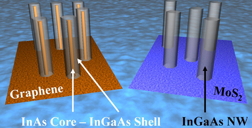
Graphic by Parsian Mohseni
Schematic representation of phase segregated InGaAs/InAs nanowires grown on graphene and single phase InGaAs nanowires grown on a different substrate
Abstract:
When a team of University of Illinois engineers set out to grow nanowires of a compound semiconductor on top of a sheet of graphene, they did not expect to discover a new paradigm of epitaxy.
Nanowires grown on graphene have surprising structure
Champaign, IL | Posted on April 22nd, 2013
The self-assembled wires have a core of one composition and an outer layer of another, a desired trait for many advanced electronics applications. Led by professor Xiuling Li, in collaboration with professors Eric Pop and Joseph Lyding, all professors of electrical and computer engineering, the team published its findings in the journal Nano Letters.
Nanowires, tiny strings of semiconductor material, have great potential for applications in transistors, solar cells, lasers, sensors and more.
"Nanowires are really the major building blocks of future nano-devices," said postdoctoral researcher Parsian Mohseni, first author of the study. "Nanowires are components that can be used, based on what material you grow them out of, for any functional electronics application."
Li's group uses a method called van der Waals epitaxy to grow nanowires from the bottom up on a flat substrate of semiconductor materials, such as silicon. The nanowires are made of a class of materials called III-V (three-five), compound semiconductors that hold particular promise for applications involving light, such as solar cells or lasers.
The group previously reported growing III-V nanowires on silicon. While silicon is the most widely used material in devices, it has a number of shortcomings. Now, the group has grown nanowires of the material indium gallium arsenide (InGaAs) on a sheet of graphene, a 1-atom-thick sheet of carbon with exceptional physical and conductive properties.
Thanks to its thinness, graphene is flexible, while silicon is rigid and brittle. It also conducts like a metal, allowing for direct electrical contact to the nanowires. Furthermore, it is inexpensive, flaked off from a block of graphite or grown from carbon gases.
"One of the reasons we want to grow on graphene is to stay away from thick and expensive substrates," Mohseni said. "About 80 percent of the manufacturing cost of a conventional solar cell comes from the substrate itself. We've done away with that by just using graphene. Not only are there inherent cost benefits, we're also introducing functionality that a typical substrate doesn't have."
The researchers pump gases containing gallium, indium and arsenic into a chamber with a graphene sheet. The nanowires self-assemble, growing by themselves into a dense carpet of vertical wires across the surface of the graphene. Other groups have grown nanowires on graphene with compound semiconductors that only have two elements, but by using three elements, the Illinois group made a unique finding: The InGaAs wires grown on graphene spontaneously segregate into an indium arsenide (InAs) core with an InGaAs shell around the outside of the wire.
"This is unexpected," Li said. "A lot of devices require a core-shell architecture. Normally you grow the core in one growth condition and change conditions to grow the shell on the outside. This is spontaneous, done in one step. The other good thing is that since it's a spontaneous segregation, it produces a perfect interface."
So what causes this spontaneous core-shell structure? By coincidence, the distance between atoms in a crystal of InAs is nearly the same as the distance between whole numbers of carbon atoms in a sheet of graphene. So, when the gases are piped into the chamber and the material begins to crystallize, InAs settles into place on the graphene, a near-perfect fit, while the gallium compound settles on the outside of the wires. This was unexpected, because normally, with van der Waals epitaxy, the respective crystal structures of the material and the substrate are not supposed to matter.
"We didn't expect it, but once we saw it, it made sense," Mohseni said.
In addition, by tuning the ratio of gallium to indium in the semiconductor ****tail, the researchers can tune the optical and conductive properties of the nanowires.
Next, Li's group plans to make solar cells and other optoelectronic devices with their graphene-grown nanowires. Thanks to both the wires' ternary composition and graphene's flexibility and conductivity, Li hopes to integrate the wires in a broad spectrum of applications.
"We basically discovered a new phenomenon that confirms that registry does count in van der Waals epitaxy," Li said.
This work was supported in part by the Department of Energy and the National Science Foundation. Postdoctoral researcher Ashkan Behnam and graduate students Joshua Wood and Christopher English also were co-authors of the paper. Li also is affiliated with the Beckman Institute for Advanced Science and Technology, the Micro and Nanotechnology Lab, and the Frederick Seitz Materials Research Lab, all at the U. of I.
NIII
One of my favorite equations in physics, is one of the earliest, force equals mass times acceleration. For objects traveling in a circle the equation is force equals mass times velocity squared divided by radius. This video is a perfect example of that equation.
http://youtu.be/dq6T5BojXc8
Courtesy of David Fuchs.
 周洪龍 金山鴻勝武舘 - 鴻勝佛家正宗
This is material coming from a space donkey.

Hung Sing Boyz, we gottit on lock down
when he's around quick to ground and pound a clown
Bruh we thought you knew better
when it comes to head huntin, ain't no one can do it better
周洪龍 金山鴻勝武舘 - 鴻勝佛家正宗
i wonder what material these space ships are made out of....

Hung Sing Boyz, we gottit on lock down
when he's around quick to ground and pound a clown
Bruh we thought you knew better
when it comes to head huntin, ain't no one can do it better
NIII
Kingston launches a 1 TB pen drive.
Damn... Moving pretty fast now. I missed that one.
 凸 囧 凸
凸 囧 凸
But it's USB 1.0 . . .
 Itinerant practitioner
This device could perform faster if you...no it can't it's an obsolete standard!
that would be something if it was usb3...or even 2...
Kung Fu is good for you.
NIII
I swear I read that it was usb 3.0, backward compatible w/ 2.0 w/ a transfer rate of something like 240/160mb....
And it's pretty expensive.
 Posting Permissions

 Reply With Quote